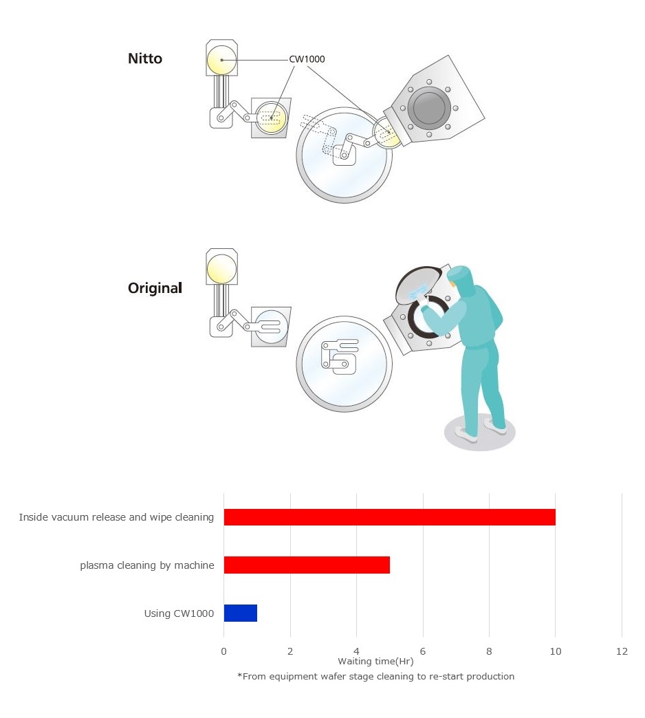
The Cleaning Wafer, having a special cleaning layer, can remove small particles in the semiconductor manufacturing equipment. Down-time of tools can be drastically reduced by using the cleaning wafer, compared with the ordinal hand cleaning method. The cleaning wafer can also be used for preventive maintenance so that yield improvement can be expected.
| Item | CW1000 |
| Structure | 
|
| Total Thickness | 720~900 (μm) |
| Surface Hardness | 500Mpa (22℃) |
| Operation Temperature | -20~50℃ ※1 |
| Size | 6inch: Oriental Flat
8/12inch: V-notch |
| Particle Type | Si, Metal (Organic) |
| Particle Size | 0.2μm and over (Measured Value) |
※1 Please consult with us if operation temperature is higher than 50°C.

|
Equipment | Effect |
| Dry Etching | Stabilize cooling helium gas | |
| Reduce maintenance time | ||
| Prober | Reduce frequency of regular maintenance | |
| Litography | Reduce vacuum error | |
| Reduce focus error | ||
| Reduce maintenance time | ||
| Ion implementation | Reduce frequency of regular maintenance | |
| Types of devices | Target | |
| Memory/Logic | Dry etcher, Lithography, Stepper | |
| Power device | Stepper, Prober | |
| Saw/Baw filter | Dry etcher, Spattering | |
| MEMS | Dry etcher |
 |
Business Hours(India time)08:30-17:00 Except for Second Sat of each month, Sun, and Holidays
TEL +91-124-4221604
Business Hours(India time)08:30-17:00
Except for Second Sat of each month, Sun, and Holidays